Mainnavigation
Subnavigation
BORDER
Pagecontent
- You are here:
- Home »
- MLDesigner »
- Examples »
- Computer Architecture »
- DLX Processor
High-Fidelity DLX Processor Architecture Model
A Complete 32 Bit Processor Simulation
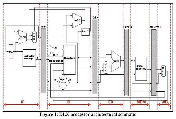
The 32-bit DLX processor architecture is a generic RISC processor designed by Hennessy & Patterson for pedagogical purposes. The DLX processor design abstracts many features of general-purpose commercial processors, and is a well-understood computer architecture. A diagram of the DLX architecture is shown below.
Functional Description
The basic DLX is a load/store architecture that features a 5-stage instruction pipeline including: instruction fetch (IF), instruction decode (ID), execution (EX), memory access (MEM) and write back (WB). The IF stage fetches 32-bit instructions from memory and manages the program counter (PC). The ID stage decodes operands, fetches values from registers, calculates branch conditionals and target addresses, detects pipeline hazards and controls the flow of program execution. The EX stage performs instruction executions for both integer and floating-point instructions and generates exceptions as needed. The MEM stage accesses data memory for load/store instructions. Finally, the WB stage is used to commit instructions, handle exceptions and store values to the register file.
The Model
The top-level diagram of a fully functional MLDesigner simulation model for the DLX processor is shown below. In addition to the ISA and pipeline architecture, the system also includes a high-fidelity model for the memory hierarchy including L1 cache and main memory. The L1 instruction cache contains 256 64-byte lines (16KB) and is directmapped and read-only. The L1 data cache contains 128 64-byte lines (8KB) and is direct- mapped with a write-through, no-write allocate strategy. The data cache also maintains cache coherency between multiple processors using a directory-based, cache-coherence protocol. Both instruction and memory caches were implemented in three different styles: non-blocking with victim buffer, blocking with victim buffer, and blocking without victim buffer. The victim buffer has 4 64-byte slots that use fully associative addressing. The model also allows for the option of running without L1 cache. Latency values for reads and writes and penalty values for misses are fully programmable. A cache miss requires that an entire block be fetched from the next lowest level in the memory hierarchy.
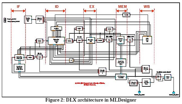
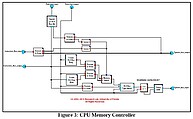
The processor model executes actual DLX machine code, typically converted from C code by a DLX compiler, which is loaded directly into memory via a text file. The value of all registers, memory locations and pipeline units can be displayed during the execution of the simulator. These values can be used to determine processor utilization, pipeline latency and throughput, instruction mix, cache miss rate and cache miss penalty. Verification of the DLX processor has been performed for all possible hazards and exceptions. Architecture tradeoffs for symmetric multiprocessor and cluster computer architectures have been simulated using this processor model. The simplicity of the top-level block diagram conceals a complex underlying hierarchical structure. Parts of the model have as may as seven layers of hierarchy. The diagram shows the structure of the CPU Memory controller module (located at the bottom of the memory section in the diagram above.)
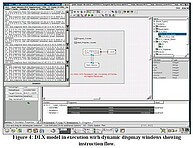
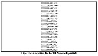
The figure above shows the top-level view of the DLX model in the MLDesigner GUI as the simulation completes. The four output windows in the upper left display the pipeline data structure at the end of each processing stage. The parameter editor window (lower left) shows the parameters used to configure the DLX system model. The "Bus Busy" data structure for the DLX system model is opened in data structure editor window (upper right) and the lower right window displays the members of that data structure. The table below shows a portion of the assembly language instruction set that is executed by the simulation. (The instruction set is read from a data file.)
Note: This model was developed by Nang Dilakanont at the HCS Lab, University of Florida, Gainesville.